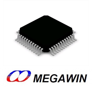
圖片僅供參考
| FLYiNG 零件編號 | ICMG32F02A064AD48MEGAWIN |
| FLYiNG 庫存現貨 | 電洽/Contact |
| 製造商 | MEGAWIN |
| 製造商零件編號 | MG32F02A064AD48 |
| 說明 | MG32F02A064AD48 MEGAWIN |
| 無鉛狀態 / RoHS 指令狀態 | RoHS |
| 訂購數量 | NTD 單價 / PCS |
| 1~9 | 39 |
| 產品類型 | ARM微控制器 - MCU |
| 製造商 | MEGAWIN |
| 原廠料號 | MG32F02A064AD48 |
| 核心 | ARM Cortex M0 |
| RoHS | RoHS |
| 安裝類型 | SMD 表面黏著式 |
| 封裝/外殼 | LQFP-48 |
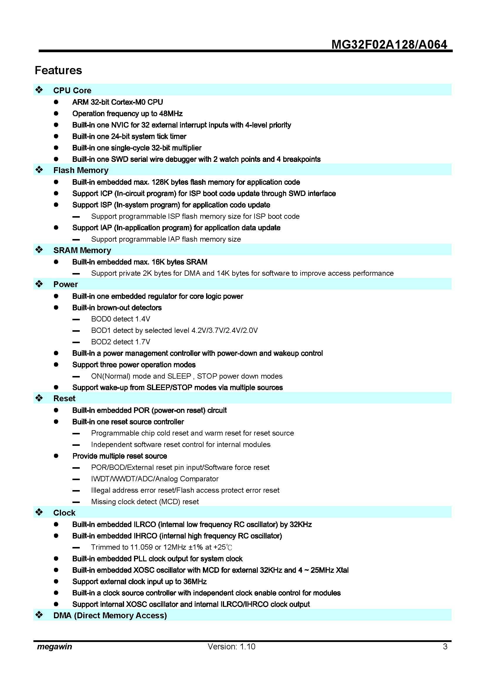
MG32F02A128/MG32F02A064
Features


Features
- CPU Core
- ARM 32-bit Cortex-M0 CPU
- Operation frequency up to 48MHz
- Built-in one NVIC for 32 external interrupt inputs with 4-level priority
- Built-in one 24-bit system tick timer
- Built-in one single-cycle 32-bit multiplier
- Built-in one SWD serial wire debugger with 2 watch points and 4 breakpoints
- Flash Memory
- Built-in embedded max. 128K bytes flash memory for application code
- Support ICP (In-circuit program) for ISP boot code update through SWD interface
- Support ISP (In-system program) for application code update
- Support programmable ISP flash memory size for ISP boot code
- Support IAP (In-application program) for application data update
- Support programmable IAP flash memory size
- SRAM Memory
- Built-in embedded max. 16K bytes SRAM
- Support private 2K bytes for DMA and 14K bytes for software to improve access performance
- Built-in embedded max. 16K bytes SRAM
- Power
- Built-in one embedded regulator for core logic power
- Built-in brown-out detectors
- BOD0 detect 1.4V
- BOD1 detect by selected level 4.2V/3.7V/2.4V/2.0V
- BOD2 detect 1.7V
- Built-in a power management controller with power-down and wakeup control
- Support three power operation modes
- ON(Normal) mode and SLEEP , STOP power down modes
- Support wake-up from SLEEP/STOP modes via multiple sources
- Reset
- Built-in embedded POR (power-on reset) circuit
- Built-in one reset source controller
- Programmable chip cold reset and warm reset for reset source
- Independent software reset control for internal modules
- Provide multiple reset source
- POR/BOD/External reset pin input/Software force reset
- IWDT/WWDT/ADC/Analog Comparator
- Illegal address error reset/Flash access protect error reset
- Missing clock detect (MCD) rese
- Clock
- Built-in embedded ILRCO (internal low frequency RC oscillator) by 32KHz
- Built-in embedded IHRCO (internal high frequency RC oscillator)
- Trimmed to 11.059 or 12MHz ±1% at +25℃
- Built-in embedded PLL clock output for system clock
- Built-in embedded XOSC oscillator with MCD for external 32KHz and 4 ~ 25MHz Xtal
- Support external clock input up to 36MHz
- Built-in a clock source controller with independent clock enable control for modules
- Support internal XOSC oscillator and internal ILRCO/IHRCO clock output
- DMA (Direct Memory Access)
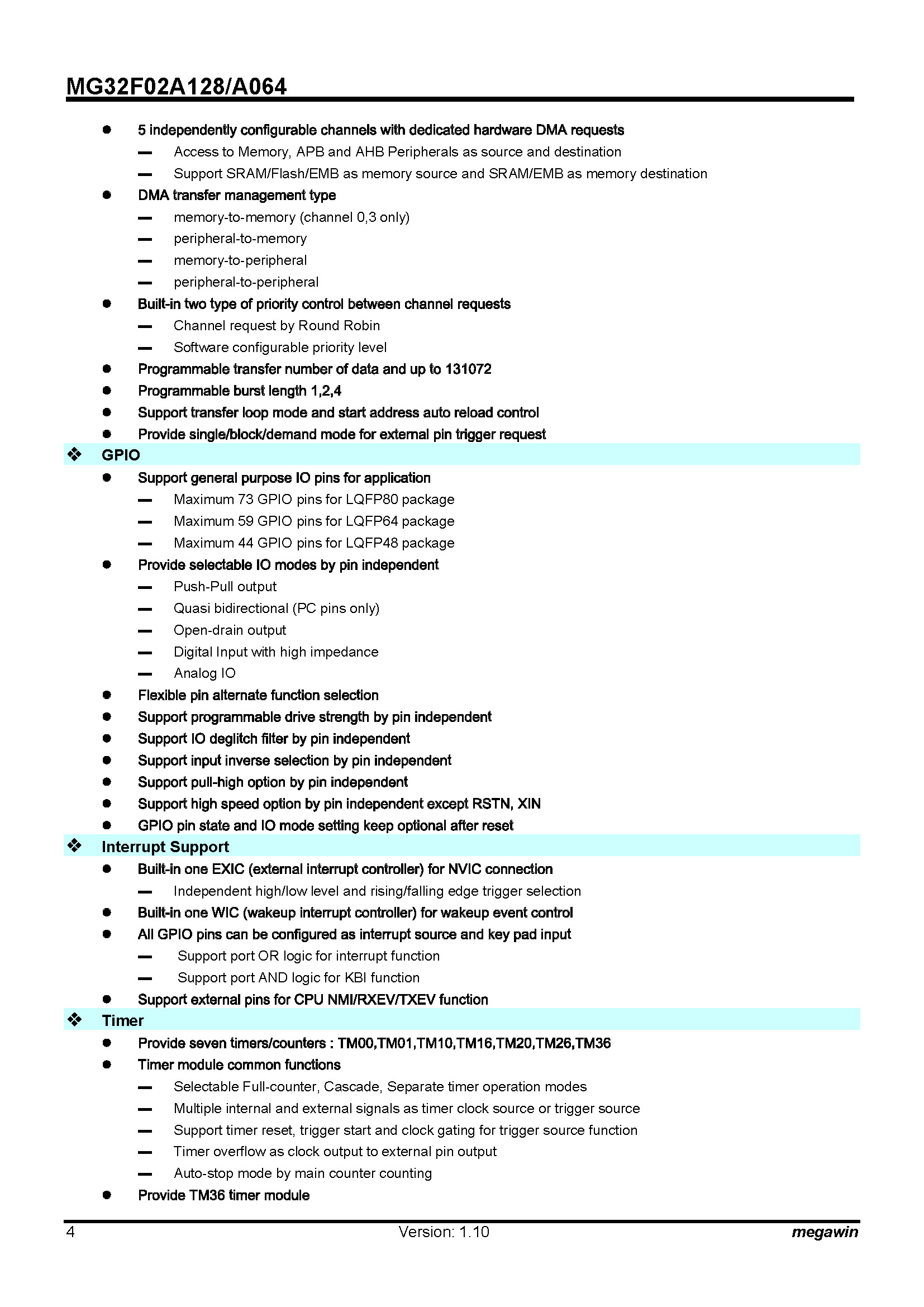
- 5 independently configurable channels with dedicated hardware DMA requests
- Access to Memory, APB and AHB Peripherals as source and destination
- Support SRAM/Flash/EMB as memory source and SRAM/EMB as memory destination
- DMA transfer management type
- memory-to-memory (channel 0,3 only)
- peripheral-to-memory
- memory-to-peripheral
- peripheral-to-peripheral
- Built-in two type of priority control between channel requests
- Channel request by Round Robin
- Software configurable priority level
- Programmable transfer number of data and up to 131072
- Programmable burst length 1,2,4
- Support transfer loop mode and start address auto reload control
- Provide single/block/demand mode for external pin trigger request
- 5 independently configurable channels with dedicated hardware DMA requests
- GPIO
- Support general purpose IO pins for application
- Maximum 73 GPIO pins for LQFP80 package
- Maximum 59 GPIO pins for LQFP64 package
- Maximum 44 GPIO pins for LQFP48 package
- Provide selectable IO modes by pin independent
- Push-Pull output
- Quasi bidirectional (PC pins only)
- Open-drain output
- Digital Input with high impedance
- Analog IO
- Flexible pin alternate function selection
- Support programmable drive strength by pin independent
- Support IO deglitch filter by pin independent
- Support input inverse selection by pin independent
- Support pull-high option by pin independent
- Support high speed option by pin independent except RSTN, XIN
- GPIO pin state and IO mode setting keep optional after reset
- Support general purpose IO pins for application
- Interrupt Support
- Built-in one EXIC (external interrupt controller) for NVIC connection
- Independent high/low level and rising/falling edge trigger selection
- Built-in one WIC (wakeup interrupt controller) for wakeup event control
- All GPIO pins can be configured as interrupt source and key pad input
- Support port OR logic for interrupt function
- Support port AND logic for KBI function
- Support external pins for CPU NMI/RXEV/TXEV function
- Built-in one EXIC (external interrupt controller) for NVIC connection
- Timer
- Provide seven timers/counters : TM00,TM01,TM10,TM16,TM20,TM26,TM36
- Timer module common functions
- Selectable Full-counter, Cascade, Separate timer operation modes
- Multiple internal and external signals as timer clock source or trigger source
- Support timer reset, trigger start and clock gating for trigger source function
- Timer overflow as clock output to external pin output
- Auto-stop mode by main counter counting
- Provide TM36 timer module
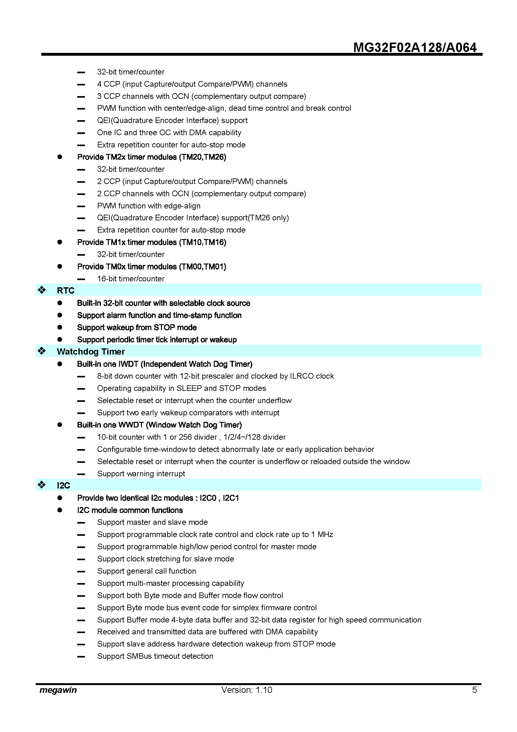
- 32-bit timer/counter
- 4 CCP (input Capture/output Compare/PWM) channels
- 3 CCP channels with OCN (complementary output compare)
- PWM function with center/edge-align, dead time control and break control
- QEI(Quadrature Encoder Interface) support
- One IC and three OC with DMA capability
- Extra repetition counter for auto-stop mode
- Provide TM2x timer modules (TM20,TM26)
- 32-bit timer/counter
- 2 CCP (input Capture/output Compare/PWM) channels
- 2 CCP channels with OCN (complementary output compare)
- PWM function with edge-align
- QEI(Quadrature Encoder Interface) support(TM26 only)
- Extra repetition counter for auto-stop mode
- Provide TM1x timer modules (TM10,TM16)
- 32-bit timer/counter
- Provide TM0x timer modules (TM00,TM01)
- 16-bit timer/counter
- RTC
- Built-in 32-bit counter with selectable clock source
- Support alarm function and time-stamp function
- Support wakeup from STOP mode
- Support periodic timer tick interrupt or wakeup
- Watchdog Timer
- Built-in one IWDT (Independent Watch Dog Timer)
- 8-bit down counter with 12-bit prescaler and clocked by ILRCO clock
- Operating capability in SLEEP and STOP modes
- Selectable reset or interrupt when the counter underflow
- Support two early wakeup comparators with interrupt
- Built-in one WWDT (Window Watch Dog Timer)
- 10-bit counter with 1 or 256 divider , 1/2/4~/128 divider
- Configurable time-window to detect abnormally late or early application behavior
- Selectable reset or interrupt when the counter is underflow or reloaded outside the window
- Support warning interrupt
- Built-in one IWDT (Independent Watch Dog Timer)
- I2C
- Provide two identical I2c modules : I2C0 , I2C1
- I2C module common functions
- Support master and slave mode
- Support programmable clock rate control and clock rate up to 1 MHz
- Support programmable high/low period control for master mode
- Support clock stretching for slave mode
- Support general call function
- Support multi-master processing capability
- Support both Byte mode and Buffer mode flow control
- Support Byte mode bus event code for simplex firmware control
- Support Buffer mode 4-byte data buffer and 32-bit data register for high speed communication
- Received and transmitted data are buffered with DMA capability
- Support slave address hardware detection wakeup from STOP mode
- Support SMBus timeout detection
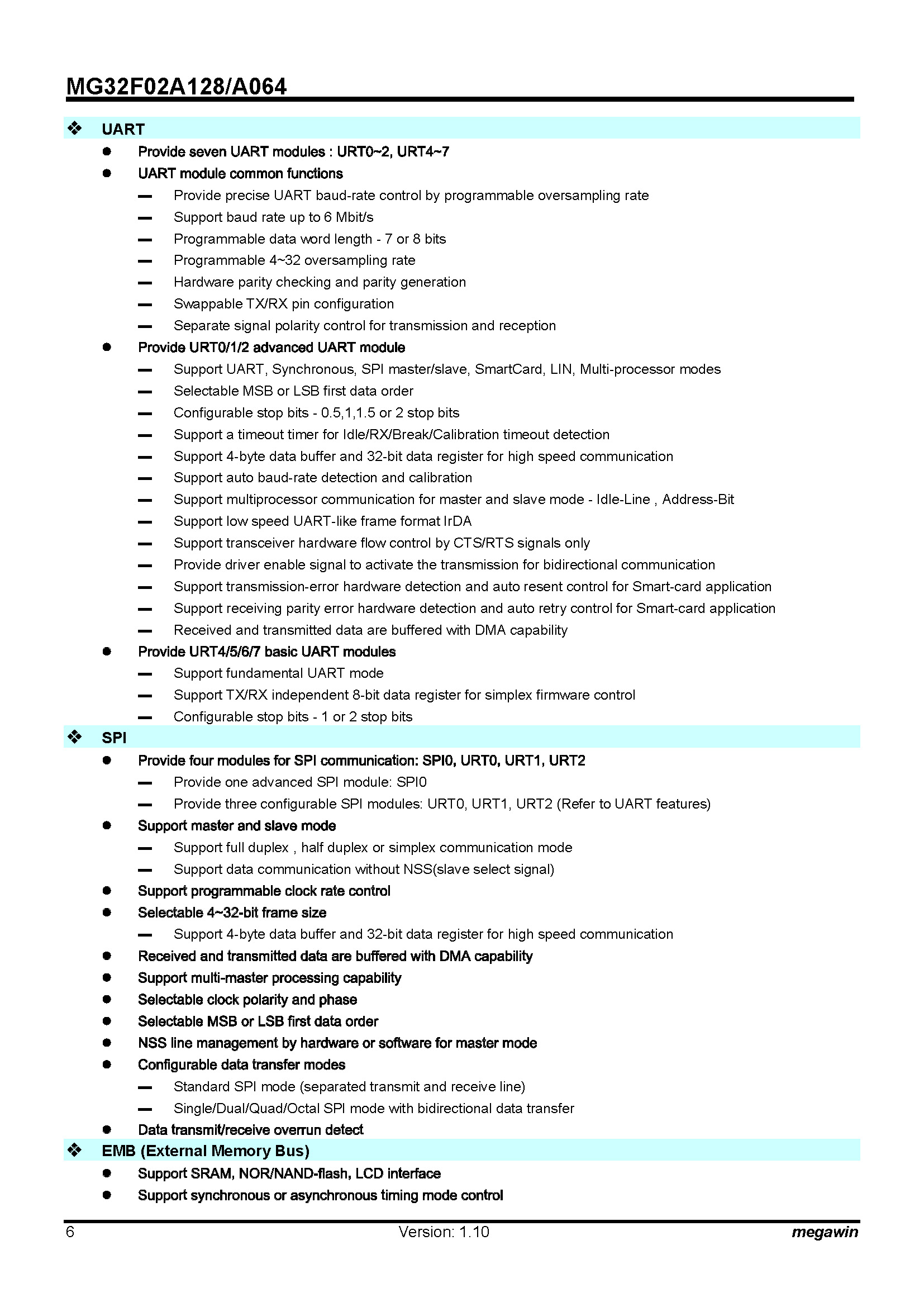
- UART
- Provide seven UART modules : URT0~2, URT4~7
- UART module common functions
- Provide precise UART baud-rate control by programmable oversampling rate
- Support baud rate up to 6 Mbit/s
- Programmable data word length - 7 or 8 bits
- Programmable 4~32 oversampling rate
- Hardware parity checking and parity generation
- Swappable TX/RX pin configuration
- Separate signal polarity control for transmission and reception
- Provide URT0/1/2 advanced UART module
- Support UART, Synchronous, SPI master/slave, SmartCard, LIN, Multi-processor modes
- Selectable MSB or LSB first data order
- Configurable stop bits - 0.5,1,1.5 or 2 stop bits
- Support a timeout timer for Idle/RX/Break/Calibration timeout detection
- Support 4-byte data buffer and 32-bit data register for high speed communication
- Support auto baud-rate detection and calibration
- Support multiprocessor communication for master and slave mode - Idle-Line , Address-Bit
- Support low speed UART-like frame format IrDA
- Support transceiver hardware flow control by CTS/RTS signals only
- Provide driver enable signal to activate the transmission for bidirectional communication
- Support transmission-error hardware detection and auto resent control for Smart-card application
- Support receiving parity error hardware detection and auto retry control for Smart-card application
- Received and transmitted data are buffered with DMA capability
- Provide URT4/5/6/7 basic UART modules
- Support fundamental UART mode
- Support TX/RX independent 8-bit data register for simplex firmware control
- Configurable stop bits - 1 or 2 stop bits
- SPI
- Provide four modules for SPI communication: SPI0, URT0, URT1, URT2
- Provide one advanced SPI module: SPI0
- Provide three configurable SPI modules: URT0, URT1, URT2 (Refer to UART features)
- Support master and slave mode
- Support full duplex , half duplex or simplex communication mode
- Support data communication without NSS(slave select signal)
- Support programmable clock rate control
- Selectable 4~32-bit frame size
- Support 4-byte data buffer and 32-bit data register for high speed communication
- Received and transmitted data are buffered with DMA capability
- Support multi-master processing capability
- Selectable clock polarity and phase
- Selectable MSB or LSB first data order
- NSS line management by hardware or software for master mode
- Configurable data transfer modes
- Standard SPI mode (separated transmit and receive line)
- Single/Dual/Quad/Octal SPI mode with bidirectional data transfer
- Data transmit/receive overrun detect
- Provide four modules for SPI communication: SPI0, URT0, URT1, URT2
- EMB (External Memory Bus)
- Support SRAM, NOR/NAND-flash, LCD interface
- Support synchronous or asynchronous timing mode control
- Support multiple types of address and data multiplex mode
- Provide optional 16/24/30-bit address mode
- Memory space 2G/32M/128K-byte for 16-bit data width
- Configurable time cycle for address latch time and data access time
- Received and transmitted data are buffered with DMA capability
- Allow running CPU code on external SRAM
- ADC
- 12-bit SAR ADC with 1.5Msps
- Configurable resolution : 12/10/8-bit
- Configurable sampling time
- Provide external 16 channels and internal 7 channels input
- Internal extra channel source : VBUF, VSSA , LDO VR0, DAC out, 1/2VDD, VPG, TS out
- Support auto-sampling and trigger by external pin, internal events and software bit
- Data alignment for output code left/right justify
- Built-in input buffer stage with bypass option
- PGA with programmable gain : 1~4
- Optional ADC top voltage reference from external VREF+ or internal IVR24
- Interrupt generation at the end of sampling, end of conversion, end of sequence conversion
- Support voltage window detection and output code limitation
- Built-in three channel independent hardware accumulators for ADC output code
- Support one-shot/channel scan/loop scan
- ADC data are buffered with DMA capability
- Support wait mode to prevent ADC overrun
- 12-bit SAR ADC with 1.5Msps
- Analog Comparator
- Provide 2 fast Rail-to-rail comparators
- Programmable 64-step threshold of internal voltage reference
- Provide external total 6 channels input for all comparators
- Two common and two independent external channels, two internal channels
- Programmable input hysteresis voltage
- Programmable response time for optimal current consumption
- Selectable compare output polarity
- Support wakeup from SLEEP and STOP modes
- Support analog watch dog as a reset source
- DAC
- One 12-bit voltage DAC
- Maximum conversion rate is 1Msps
- Conversion start trigger by register written, external pin and internal events
- Build in internal output buffer
- Data alignment for input code left/right justify
- Configurable code width : 12/10/8-bit
- Output data are buffered with DMA capability
- One 12-bit voltage DAC
- Temperature Sensor
- Built-in a temperature sensor in ADC macro
- Temperature resolution : +/- 2 °C (Typical)
- Temperature operation range : -40°C ~ 125°C
- GPL (General Purpose Logic)
- Support data inverse, bit order change, byte order change and parity check
- Data bit order change for 8/16/32-bit reverse
- Data byte order change between Little endian and Big endian for 16/32-bit range
- Parity Check for 8/16/32 bit range
- Support CRC (Cyclic Redundancy Check) calculation
- Programmable CRC initial value
- CRC output bit order change
- CRC with fixed common polynomial
- CRC8 polynomial 0x07
- CRC16 polynomial 0x8005
- CCITT16 polynomial 0x1021
- CRC32(IEEE 802.3) polynomial 0x4C11DB7
- Support signed/unsigned 32-bit divider
- Operation in 8 clock cycles
- Input data are buffered with DMA capability
- Support data inverse, bit order change, byte order change and parity check
- Misc.
- Timer synchronous enable global control
- OBM(Output Signal Break and Modulation) control
- Support two sets of OBM for output signal break and modulation control
- NCO(Numerically Controlled Oscillator) output with FDC and PF modes
- Support two sets of CCL(Configurable Custom Logic)
- 32-bit non-reset backup register
- Provide on chip 16 bytes Unique ID code
- Operating
- Operating voltage range 1.8V ~ 5.5V
- Operating temperature range -40℃ ~ 105℃ (**1)
- Operating frequency range up to 48MHz
- Package Types
- LQFP80 / LQFP64 / LQFP48
