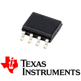
| FLYiNG 零件編號 | ICTLC27L2CDRTI |
| FLYiNG 庫存現貨 | 電洽/Contact |
| 製造商 | TEXAS INSTRUMENTS |
| 製造商零件編號 | TLC27L2CDR |
| 說明 | TLC27L2CDR SOIC-8 TI |
| 無鉛狀態 / RoHS 指令狀態 | RoHS |
| 訂購數量 | NTD 單價 / PCS |
| 1~9 | 120 |
| 10~24 | 100 |
| 25~99 | 70 |
| 100~249 | 60 |
| 250~500 | 55 |
| 500~ | 50 |
| 半導體 | High Speed Operational Amplifiers 高速運算放大器 |
| 製造商 | TEXAS INSTRUMENTS |
| 系列 | LinCMOS Precision Dual Operational Amplifiers |
| 原廠料號 | TLC27L2CDR |
| 說明 | TLC27L2CDR SOIC-8 TI |
| 電路數 | 2 |
| 增益帶寬積(GBP) | 110 kHz |
| 迴轉率(SR) | 0.03V/µs |
| 每通道輸出電流 | 30 mA |
| 輸入偏壓電流(Ib) | 0.6 pA |
| 輸入偏移電壓(Vos) | 1.1 mV |
| 工作電壓 | 3~16V |
| 工作溫度 | 0℃ ~70℃ |
| 安裝類型 | SMD |
| 封裝/外殼 | SOIC-8 |
| 標準包裝 | 75 pcs/tube |
文件:TLC27L2,TLC27L2A,TLC27L2B,TLC27L7.png)
TLC27L2,TLC27L2A,TLC27L2B,TLC27L7
Feature
Description
TLC27L2, TLC27L2A, TLC27L2B, TLC27L7
特點
.png)
TLC27L2,TLC27L2A,TLC27L2B,TLC27L7
Feature
- Trimmed Offset Voltage: TLC27L7...500 µV Max at 25°C, VDD = 5 V
- Input Offset Voltage Drift . . . Typically 0.1 µV/Month, Including the First 30 Days
- Wide Range of Supply Voltages Over Specified Temperature Range:>
- 0°C to 70°C...3 V to 16 V
- -40°C to 85°C...4 V to 16 V
- -55°C to 125°C...4 V to 16 V
- Single-Supply Operation
- Common-Mode Input Voltage Range Extends Below the Negative Rail (C-Suffix, I-Suffix Types)
- Ultra-Low Power...Typically 95 µW at 25°C, VDD = 5 V
- Output Voltage Range Includes Negative Rail
- High Input Impedance...1012 Typ
- ESD-Protection Circuitry
- Small-Outline Package Option Also Available in Tape and Reel
- Designed-In Latch-Up immunity
- LinCMOS is a trademark of Texas Instruments.
Description
The TLC27L2 and TLC27L7 dual operational amplifiers combine a wide range of input offset voltage grades with low offset voltage drift, high input impedance, extremely low power, and high gain.
These devices use Texas Instruments silicon-gate LinCMOS™ technology, which provides offset voltage stability far exceeding the stability available with conventional metal-gate processes.
The extremely high input impedance, low bias currents, and low power consumption make these cost-effective devices ideal for high gain, low frequency, low power applications. Four offset voltage grades are available (C-suffix and I-suffix types), ranging from the low-cost TLC27L2 (10 mV) to the high-precision TLC27L7 (500 µV). These advantages, in combination with good common-mode rejection and supply voltage rejection, make these devices a good choice for new state-of-the-art designs as well as for upgrading existing designs.
In general, many features associated with bipolar technology are available in LinCMOS™ operational amplifiers, without the power penalties of bipolar technology. General applications such as transducer interfacing, analog calculations, amplifier blocks, active filters, and signal buffering are easily designed with the TLC27L2 and TLC27L7. The devices also exhibit low voltage single-supply operation and ultra-low power consumption, making them ideally suited for remote and inaccessible battery-powered applications. The common-mode input voltage range includes the negative rail.
A wide range of packaging options is available, including small-outline and chip-carrier versions for high-density system applications.
The device inputs and outputs are designed to withstand -100-mA surge currents without sustaining latch-up.
The TLC27L2 and TLC27L7 incorporate internal ESD-protection circuits that prevent functional failures at voltages up to 2000 V as tested under MIL-STD-883C, Method 3015.2; however, care should be exercised in handling these devices as exposure to ESD may result in the degradation of the device parametric performance.
The C-Suffix devices are characterized for operation from 0°C to 70°C. The I-suffix devices are characterized for operation from -40°C to 85°C. The M-suffix devices are characterized for operation over the full military temperature range of -55°C to 125°C.
TLC27L2, TLC27L2A, TLC27L2B, TLC27L7
特點
- 修整偏移電壓:TLC27L7...最大500 µV,於25°C,VDD = 5 V
- 輸入偏移電壓漂移:典型0.1 µV/月,包括前30天
- 寬供電電壓範圍(在指定溫度範圍內):
- 0°C至70°C...3 V至16 V
- -40°C至85°C...4 V至16 V
- -55°C至125°C...4 V至16 V
- 單電源操作
- 共模輸入電壓範圍:延伸至負電源以下(C型和I型)
- 超低功耗:典型95 µW於25°C,VDD = 5 V
- 輸出電壓範圍:包括負電源
- 高輸入阻抗:典型值10^12Ω
- ESD保護電路
- 可選小型輪廓封裝,也可提供卷帶包裝
- 設計防止鎖定現象
- LinCMOS™技術是德州儀器的商標
TLC27L2和TLC27L7雙運算放大器結合了多種輸入偏移電壓等級,具有低偏移電壓漂移、高輸入阻抗、極低功耗和高增益。這些器件採用德州儀器的矽閘LinCMOS™技術,提供的偏移電壓穩定性遠超傳統金屬閘工藝。
極高的輸入阻抗、低偏置電流和低功耗使這些具成本效益的器件成為高增益、低頻率、低功耗應用的理想選擇。提供四種偏移電壓等級(C型和I型),從低成本的TLC27L2(10 mV)到高精度的TLC27L7(500 µV)。這些優勢,加上良好的共模抑制比和電源電壓抑制比,使這些器件成為新型設計的良好選擇,也適合升級現有設計。
一般而言,與雙極性技術相關的許多特性都可以在LinCMOS™運算放大器中找到,而無需承擔雙極性技術的功耗懲罰。TLC27L2和TLC27L7非常適合設計傳感器接口、模擬計算、放大器模塊、有源濾波器和信號緩衝器等應用。這些器件還具有低電壓單電源操作和超低功耗,非常適合遠程和難以接近的電池供電應用。共模輸入電壓範圍包括負電源。
提供多種封裝選擇,包括小型輪廓和芯片載體版本,以滿足高密度系統應用的需求。器件的輸入和輸出設計能承受-100 mA的浪湧電流而不會鎖定。TLC27L2和TLC27L7內部集成了ESD保護電路,可防止在最高2000V下的功能故障(根據MIL-STD-883C,方法3015.2測試),但在處理這些器件時仍需小心,以免暴露於ESD會導致器件參數性能下降。
C型器件的操作溫度範圍為0°C至70°C。
I型器件的操作溫度範圍為-40°C至85°C。
M型器件的操作溫度範圍為-55°C至125°C。


