

| FLYiNG 零件編號 | IC74HC138D653NEXPERIA |
| FLYiNG 散料庫存 | 電洽/Contact |
| FLYiNG 標準包裝庫存 | 電洽/Contact |
| 製造商 | NEXPERIA |
| 製造商零件編號 | 74HC138D,653 |
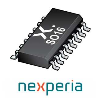
| 說明 | 74HC138D,653 SO-16 NEXPERIA |
| 無鉛狀態 / RoHS 指令狀態 | RoHS |
| 積體電路類型 | CMOS IC |
| 輸入行數 | 3 Input |
| 輸出行數 | 8 Output |
| 輸出電流 | -5.2~5.2 mA |
| 傳播延遲時間 | 50nS |
| 電源電壓 | 2~6 V |
| 工作溫度 | -40~125°C |
| 封裝/外殼 | SO-16 |
| 安裝類型 | SMD 表面黏著式 |
| 標準包裝數量 | 2500/REEL |
文件:74HC136; 74HCT138.png)
74HC138; 74HCT138
3-to-8 line decoder/demultiplexer; inverting
General description
Features and benefits
74HC138; 74HCT138
3-to-8 line decoder/demultiplexer; inverting
General description
The 74HC138; 74HCT138 decodes three binary weighted address inputs (A0, A1 and A2) to eight mutually exclusive outputs (Y0 to Y7). The device features three enable inputs (E1, E2 and E3). Every output will be HIGH unless E1 and E2 are LOW and E3 is HIGH. This multiple enable function allows easy parallel expansion to a 1-of-32 (5 to 32 lines) decoder with just four '138 ICs and one inverter. The '138 can be used as an eight output demultiplexer by using one of the active LOW enable inputs as the data input and the remaining enable inputs as strobes. Inputs include clamp diodes. This enables the use of current limiting resistors to interface inputs to voltages in excess of VCC.
Features and benefits
- Wide supply voltage range from 2.0 to 6.0 V
- CMOS low power dissipation
- High noise immunity
- Latch-up performance exceeds 100 mA per JESD 78 Class II Level B
- Demultiplexing capability
- Multiple input enable for easy expansion
- Ideal for memory chip select decoding
- Active LOW mutually exclusive outputs
- Input levels:
- For 74HC138: CMOS level
- For 74HCT138: TTL level
- Complies with JEDEC standards:
- JESD8C (2.7 V to 3.6 V)
- JESD7A (2.0 V to 6.0 V)
- ESD protection:
- HBM: ANSI/ESDA/JEDEC JS-001 class 2 exceeds 2000 V
- CDM: ANSI/ESDA/JEDEC JS-002 class C3 exceeds 1000 V
- Multiple package options
- Specified from -40 °C to +85 °C and from -40 °C to +125 °C
74HC138; 74HCT138
3-to-8 線解碼器/解多工器(反向輸出)
一般描述
74HC138 和 74HCT138 可將三個二進制加權位址輸入(A0、A1 和 A2)解碼為八個互斥輸出(Y0 至 Y7)。該元件具有三個使能輸入(E1、E2 和 E3)。所有輸出預設為高電位(HIGH),除非 E1 和 E2 為低電位(LOW),且 E3 為高電位(HIGH)。這種多重使能功能允許透過四顆 74HC138 和一顆反相器,輕鬆擴展為 1-32(5-to-32 線)解碼器。
74HC138 也可作為 8 輸出解多工器,方法是將其中一個有效低(ACTIVE LOW)的使能輸入用作數據輸入,而其餘的使能輸入用作鎖存信號(strobe)。該元件的輸入端包含箝位二極體,因此可透過限流電阻與高於 VCC 的電壓相連接。
特點與優勢
- 寬電源電壓範圍:2.0V 至 6.0V
- CMOS 低功耗設計
- 高抗噪能力
- Latch-up 抑制能力超過 100mA(符合 JESD 78 Class II Level B)
- 具備解多工(demultiplexing)功能
- 多重輸入使能,便於擴展
- 適用於記憶體晶片選擇解碼
- 主動低(Active LOW)互斥輸出
- 輸入電平:
- 74HC138:CMOS 電平
- 74HCT138:TTL 電平
- 符合 JEDEC 標準:
- JESD8C(2.7V 至 3.6V)
- JESD7A(2.0V 至 6.0V)
- ESD 保護等級:
- HBM(人體模型):符合 ANSI/ESDA/JEDEC JS-001 Class 2,超過 2000V
- CDM(充電裝置模型):符合 ANSI/ESDA/JEDEC JS-002 Class C3,超過 1000V
- 多種封裝選擇
- 工作溫度範圍:-40°C 至 +85°C,部分型號可達 -40°C 至 +125°C